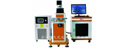

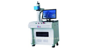
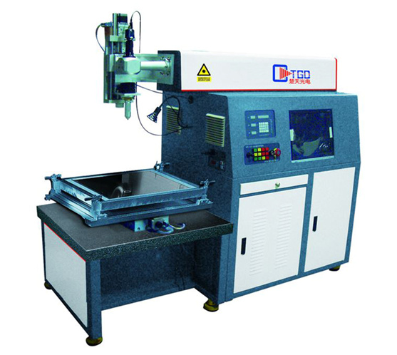


Superiority analysis of LED laser scribing
Compared with the traditional mechanical characterization, the scribing lines of LED are much narrower, so the utilization ratio of materials is improved remarkably, so the output efficiency is improved. The other is a non-contact laser processing technology, characterization of micro cracks and other damage to the wafer is smaller, the closer the wafer between particles, high efficiency, high output capacity, and reliability of LED devices also greatly improve product.
Specifically, laser machining is a non-contact processing, as an alternative to traditional technology of mechanical cutting, laser scribing incision is very small, after focusing laser micro spot effect on the surface of the wafer, the rapid gasification of materials, manufacturing of very small incision between the active region of the LED, which can cut more LED monomers in the limited area on wafer. The laser scribing is particularly good at, on GaAs and other brittle compound semiconductor wafer materials it is understood that the laser processing of LED wafer, the thickness of the substrate is typical of scratching depth 1/3 to 1/2, which can get segmentation faults are very clean, making the narrow and deep Laser Scratching cracks at the same time to ensure high speed. At the same time. This requires, laser with narrow pulse width, high beam quality, high peak power, high repetition rate and excellent quality.
Of course, not all lasers are suitable for LED scribing, and the main reason is the transmission of laser light to visible wavelengths by wafer materials. However, compared with the traditional blade cutting, laser engraving the crystal cracks and micro crack expansion is greatly reduced, LED monomer closer laser scribing, not only improves the production efficiency, and improve the processing speed, avoid the blade wear processing defects and cost loss, in short, high precision laser machining, machining tolerance, low cost.